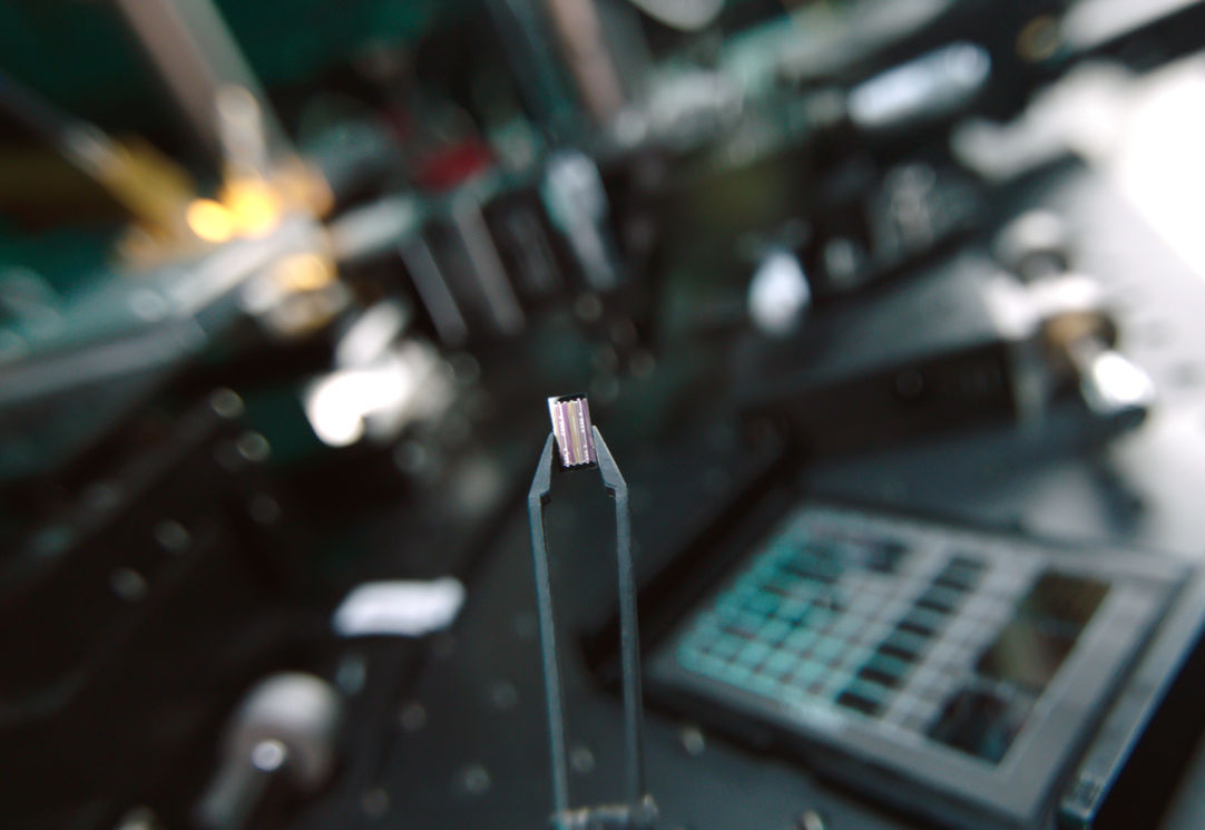
Advanced TFLN Photonic Chip Manufacturing Technology
Our Expertise in Cutting-Edge Manufacturing
Our state-of-the-art proprietary technology is designed to cater to both fabless companies, which are early adopters of next-generation photonic chips, and conventional silicon photonic foundries looking to enhance their platforms by integrating TFLN. It encompasses a range of advanced manufacturing capabilities, including:
-
Precision TFLN Micromachining
-
Multilayer Metallization
-
Cladding and Layer Openings
-
Device-layer undercut
These processes allow for the realization of various on-chip components and functionalities:
-
Electro-Optic Modulators for fast communication.
-
CMOS Compatibility for easy integration.
-
Low-Loss Fiber Coupling for reliable connectivity.
-
Frequency Conversion via PPLN for spectroscopy, optical and quantum computations.
-
Acousto-Optic Modulation for dynamic light control.
-
Efficient interfacing for hybrid and heterogeneous integration with Silicon Photonics.

Driving Forces Behind Next-Generation Photonic Integrated Circuits

High Bandwidth
Supporting AI, HPC, 5G/6G, and cloud computing with ultra-fast, energy-efficient interconnects and data rates beyond 400 Gbit/s.

Large-Scale Integration
Compact, low-loss solutions with heterogeneous integration, photonic-electronic co-integration, and programmable PICs.

Low Power Consumption
Efficient systems with CMOS-level voltage operation and low-loss waveguides, versatile packaging, and minimal thermal effects.

Wide Wavelength Range
Expanding optical data links and enabling quantum computing, biosensing, and spectroscopy.

New Functionalities
Advanced features like on-chip wavelength conversion, isolators, and ultra-fast photodetectors.
TFLN: A Versatile PIC Platform for the Future

High Nonlinearity
Exceptional for efficient modulation and wavelength conversion.

Robustness and Reliability
Proven telecom material for decades, ensuring durability in harsh environments with scalable integration.

Low Optical Loss
Enables large-scale on-chip circuits, delay lines, and minimizes the need for optical amplifiers.

Compact Footprint
Ensuring large number of components per chip area, delivers high performance in a miniaturized format.

Wide Transparency
Operates across a broad wavelength range, supporting telecom, quantum, and more.

Piezoelectric Effect
Supports photon-phonon interactions and enables various transducer applications.
Further Reading
-
Lithium niobate photonics: Unlocking the electromagnetic spectrum
-
Photonic Crystal Cavity IQ Modulators in Thin-Film Lithium Niobate
-
An integrated photonic engine for programmable atomic control
-
Integrated lithium niobate electro-optic modulators operating at CMOS-compatible voltages
-
Design rules for frequency conversion in periodically poled thin film lithium niobate waveguides
-
Broadband electro-optic frequency comb generation in a lithium niobate microring resonator
-
Stable and compact RF-to-optical link using lithium niobate on insulator waveguides
Empowering PIC Designers with PDKs
We provide standardized Process Design Kits (PDKs) that streamline product development for photonic integrated circuit (PIC) designers, enabling faster design processes and comprehensive sanity checks. Our expertise guides designers through each stage of the chip design process. Additionally, our PDKs are continuously improved through regular updates, enhancing their reliability and functionality for future designs.

Photonic Designer

TFLN Chips
Design Rules
Models & Statistic
Technology Layers


TFLN PIC FOUNDRY
Process Design Kit
Wafer-scale Manufacturing

End Users
Tapeout


